Full Guide on FMC STM32:SDRAM Integration
Oct 13, 2025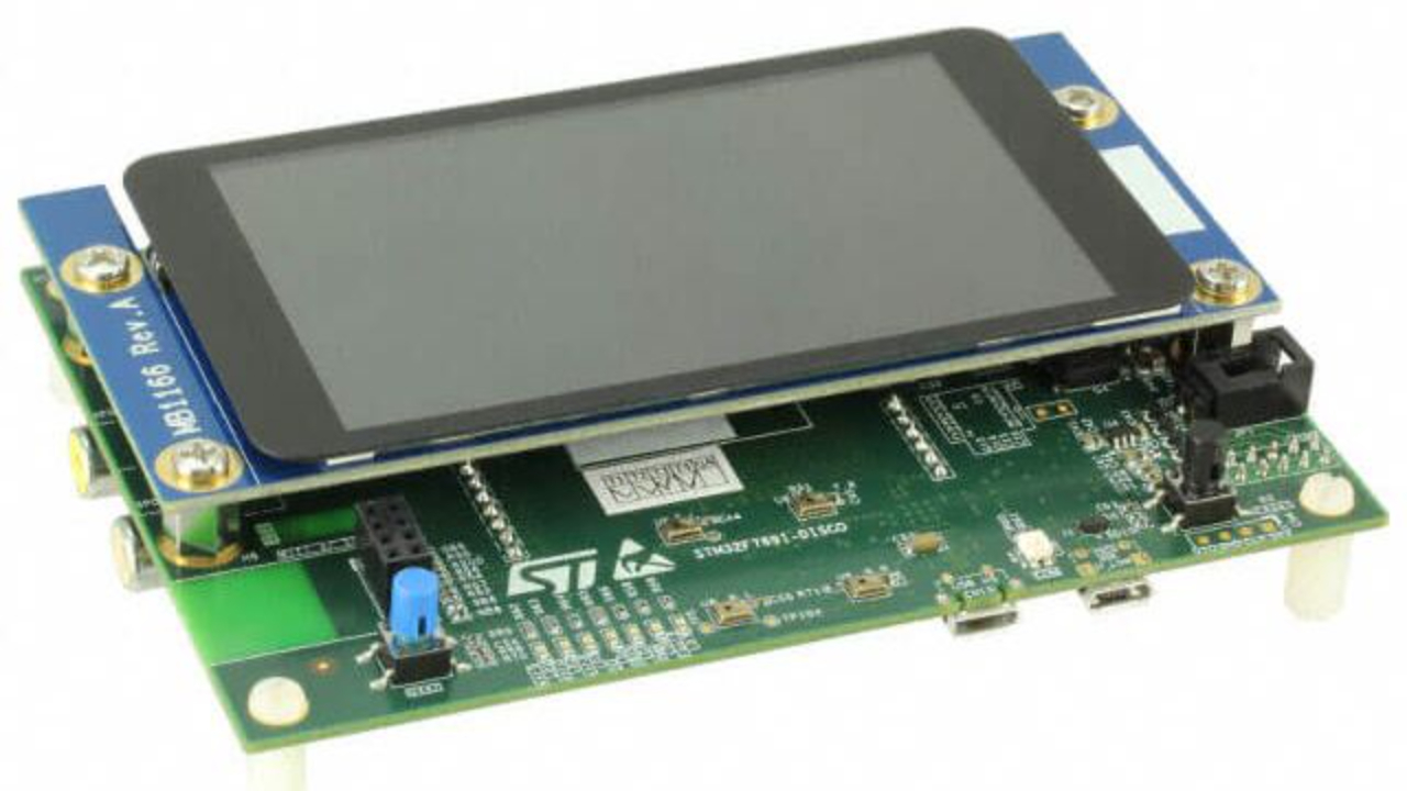
While STM32 microcontrollers offer enough RAM for various embedded applications, there are scenarios—such as image processing—where additional memory is required. In these cases, having an additional memory unit is essential for storing large amounts of frame data, ensuring the smooth operation of resource-intensive applications. In this guide, we delve into STM32 SDRAM integration to provide the microcontroller with additional memory. For that purpose, we will cover configuring the FMC Interface using the STM32CubeMX graphical tool and provide a simple example of accessing SDRAM via the FMC Interface.
Hardware
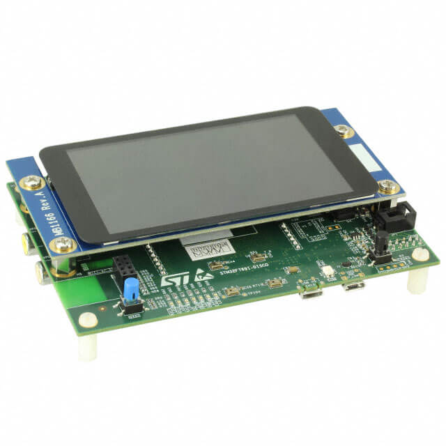
In this tutorial, I use the STM32F769 Discovery Board. This board already incorporates a 16-MByte SDRAM memory (IS42S32400F) and the necessary wiring. However, this tutorial applies to other SDRAM memory units with small modifications. Additional resources on the hardware and firmware are provided at the end of the article.
FMC SDRAM CubeMX configuration
First, we configure the Flexible Memory Controller (FMC) using the STM32CubeMx Graphical Tool. Within the connectivity, choose FMC and SDRAM among different options as shown in the picture below.
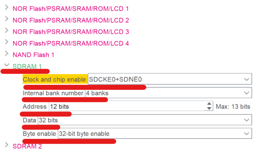
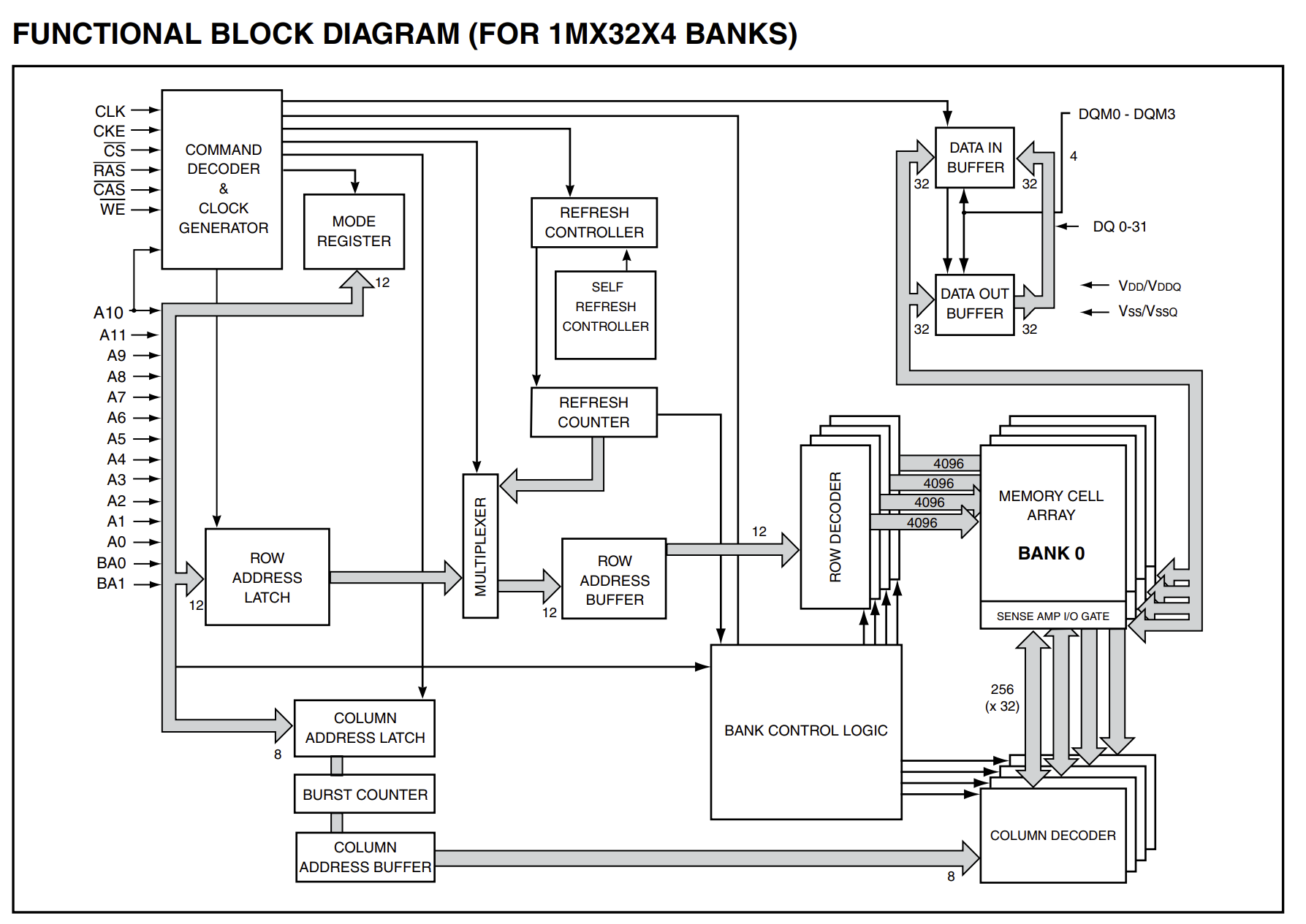
Then, we have to specify the number of banks, address bits, and data bits. You can use the datasheet of the SDRAM unit you are using to find these specifications. For example, in my case, IS42S32400F memory has the following characteristics:
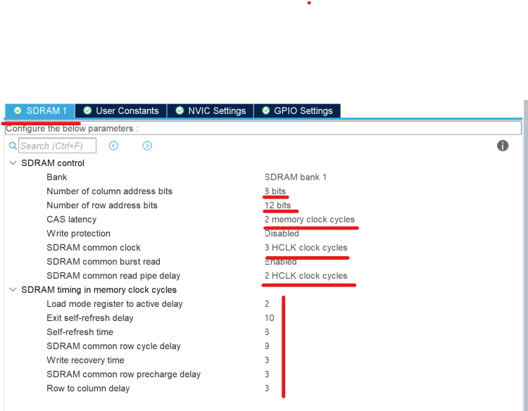
Once we have specified these general parameters, an additional window (SDRAM 1) will pop up to configure even finer details of the protocol. Again, using the blog diagram, we can define the number of column address bits and row address bits. Next in turn is CAS (Column address strobe) latency which defines the time takes for a memory unit to prepare the data to be read. In my case, I set its value to 2.
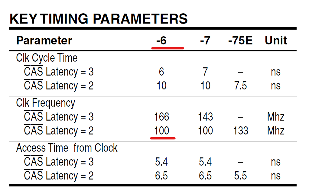
Another important thing is to set the operating frequency of the FMC protocol. It is essential to set the frequency below a frequency specified in the datasheet. As shown in the picture below, the maximum frequency is 100 MHz for CAS equal to 2.
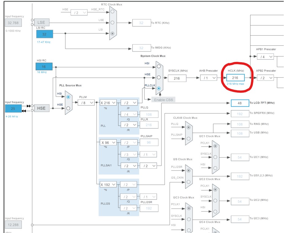
In my microcontroller, FMC is driven by the HCLK. In some cases, the FMC is driven by a separate block which will require configuring its clock. In the SDRAM control configuration, I set the common clock to 3 HCLK clock cycles, resulting in a 72 MHz frequency, because HCLK frequency is 216 MHZ as shown in the figure below.
The next important is to set up SDRAM timing details. For that purpose, I used the datasheet of the memory unit. Other than that, the specifications in the datasheet have to be converted into clock cycles. Considering a 72 MHz clock, I obtained the following values:
1. Load mode register (tmrd): 14 ns - 2 clock cycles.
2. Exit self-refresh delay(txsr): 70 ns - 10 clock cycles.
3. Self-refresh time (tras): 42 ns - 6 clock cycles
4. SDRAM common row cycle delay (trc) - 9 clock cycles
5. Write recovery time(tdpl) - 2 clock cycles
6. SDRAM common row precharge delay(trp) - 3 clock cycles
7. Row to column delay(trcd) - 3 clock cycles
After all these steps, I obtained the following configurations:
Finally, we can save this file and generate code. The next great deal is to find a memory bank corresponding to SDRAM 1. We refer to the reference manual of the MCU we are using to find this information: just search for ’FMC memory bank’ and you should find a table similar to the one presented below.
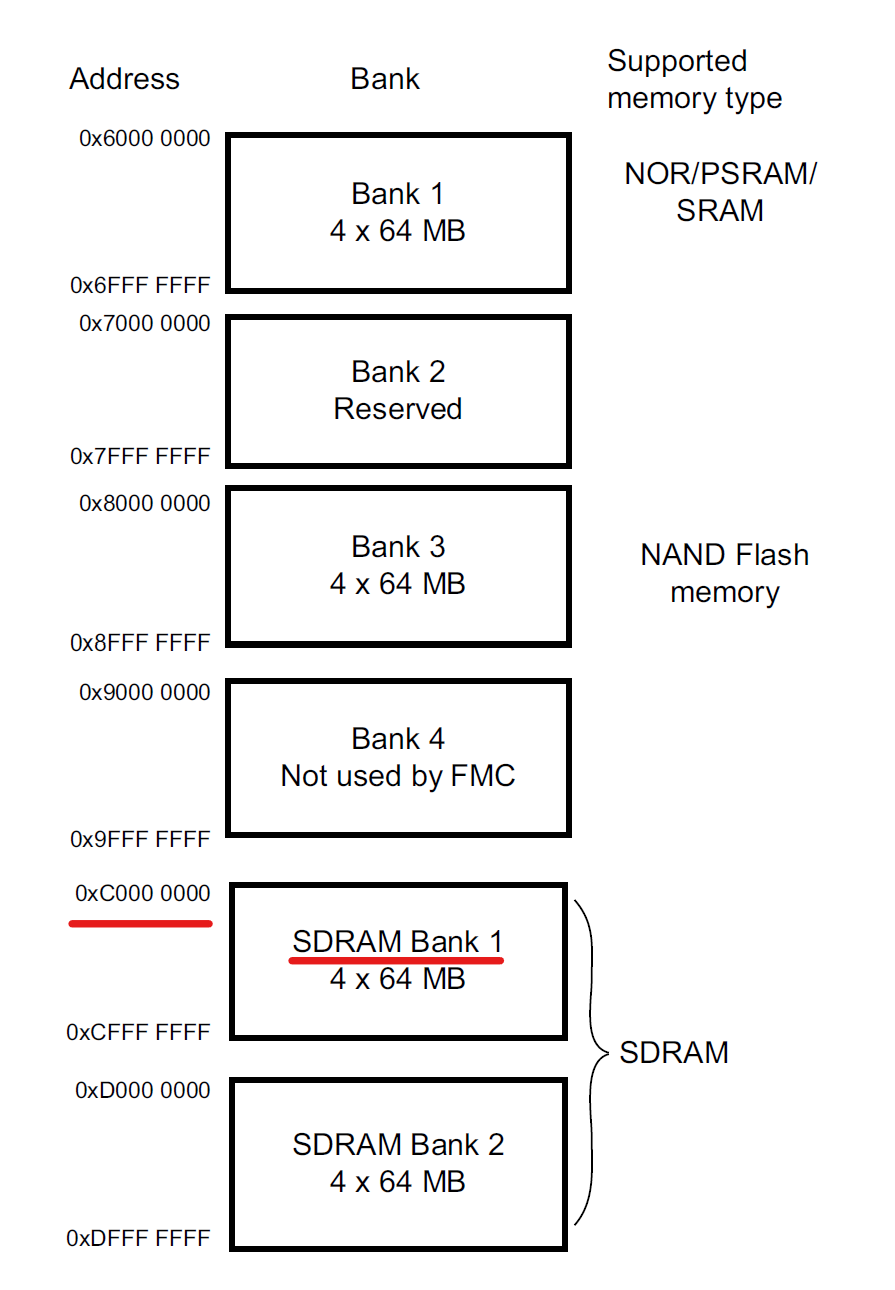
From this table, we find that 0xC0000000-0xCFFFFFFF is an address range of SDRAM 1. So, whenever we store data within this range, it will be automatically stored inside the SDRAM memory unit. To test it, I added the following code to my project:
// outside the main function
#define SDRAM_START_ADDRESS 0xC0000000
// inside the main function, after peripherals configuration:
for(int i = 0; i< 256;i++)
{
    *(__IO uint8_t*)(SDRAM_START_ADDRESS + i) = i;
}
After all these steps, the STM32 MCU has an additional 16 MB of Memory space to store images and other data.