STM32 CAN Bus Tutorial P2, Loopback Mode and Configuration
Oct 13, 2025
So, let's continue our endeavor to understand and implement the STM32 CAN BUS. If you miss the first part of the tutorial, please refer to the following links:
The 1st and 3rd parts of the tutorial are available:
https://www.steppeschool.com/blog/stm32-can-interface-theory
https://www.steppeschool.com/blog/stm32-can-bus-tutorial-p3
The Source Code:
https://www.steppeschool.com/stm32-can-bus-course
After passing the tedious theoretical part of the CAN journey, we finally cover the practical aspects of the CAN Interface. In this part of the tutorial, we will configure the STM32 CAN Peripheral and test it in loopback mode.
First, we need to create a new project and open the.IOC file of the project. Within Connectivity, choose the CAN Interface. I am sure you can handle all these steps. Otherwise, I will highly recommend the STM32 Programming Course for beginners:
STM32 CAN Operating Modes
If you open the parameter setting, you notice that there are several operating modes of the CAN Interface: Normal, Restricted Operation, Bud Monitoring, External Loopback, and Internal Loopback.
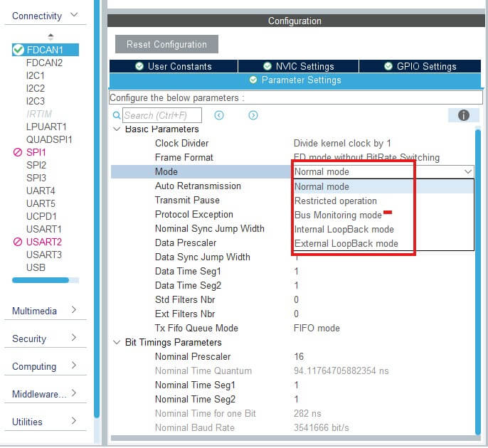
Normal Mode, as its name suggests, is the standard communication mode, in which CAN can transmit and receive data.
In Restricted Operation mode, on the other hand, the MCU can only receive the remote frames. It has other peculiarities:
-
It can acknowledge valid frames.
-
It does not send data frames, remote frames, active error frames, or overload frames.
-
In case of error or overload conditions, it does not send dominant bits.
-
Instead, it waits for a bus-idle condition to resynchronize with CAN communication.
-
Restricted Operation Mode is automatically entered when the Tx handler cannot read data from the message RAM in time.
To leave this mode, the software must clear the ASM bit of the FDCAN_CCCR register.
This mode can be used in applications that adapt to different CAN bit rates. The application tests different bit rates. It leaves Restricted Operation Mode once a valid frame is received.
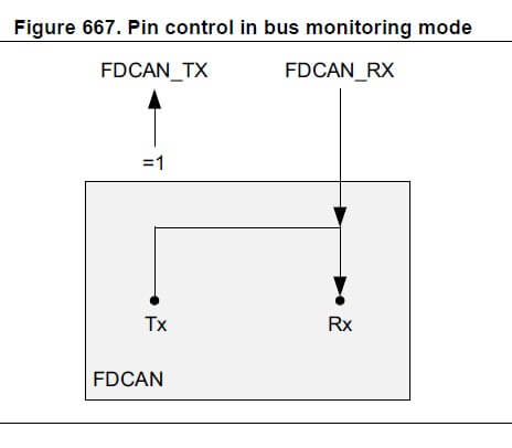
The Figure below explains the Bus Monitoring Mode clearly. This mode is useful in analyzing the bus without affecting it. Since Tx and Rx lines are connected internally, it can also be used to monitor its own frames without really transmitting them.
Finally, we have External and internal loop-back nodes, which we primarily use for testing. In external loop-back mode, the FDCAN treats its own transmitted messages as received messages and stores them (if they pass acceptance filtering) into Rx FIFOs. This mode is provided for hardware self-test. To be independent from external stimulation, the FDCAN ignores acknowledged errors (recessive bit sampled in the acknowledge slot of a data/remote frame) in loop-back mode.
Internal loop-back mode can be used for a “hot self-test”, meaning the FDCAN can be tested without affecting a running CAN system connected to the FDCAN_TX and FDCAN_RX pins. In this mode, the FDCAN_RX pin is disconnected from the FDCAN and FDCAN_TX pin is held recessive.
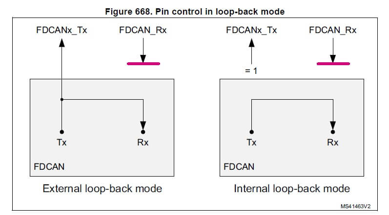
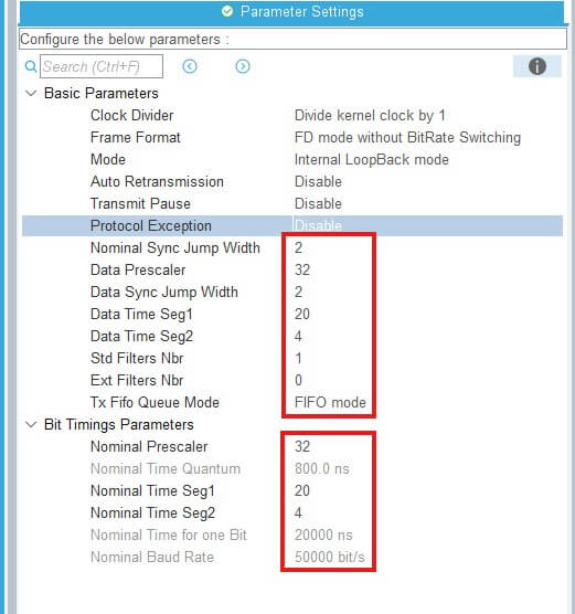
In this tutorial, we will use Internal Loopback Mode to test the CAN Interface without additional hardware.
STM32 CAN/FDCAN Bit Timings
The next on the to-do list is configuring the CAN Clock and bit timings. Let's look at the clock Configuration of the STM32G491 in my project. In your case, it could be slightly different. Pay attention to the PLLQ output, which has a frequency of 40 MHz.
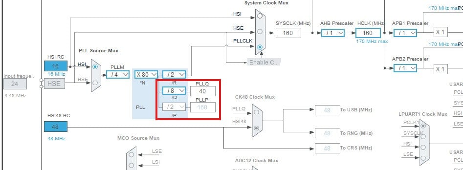
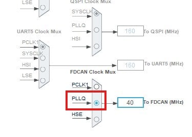
If you scroll, you will find a field to choose the CAN Peripheral Clock Source. I chose PLLQ as the clock input.
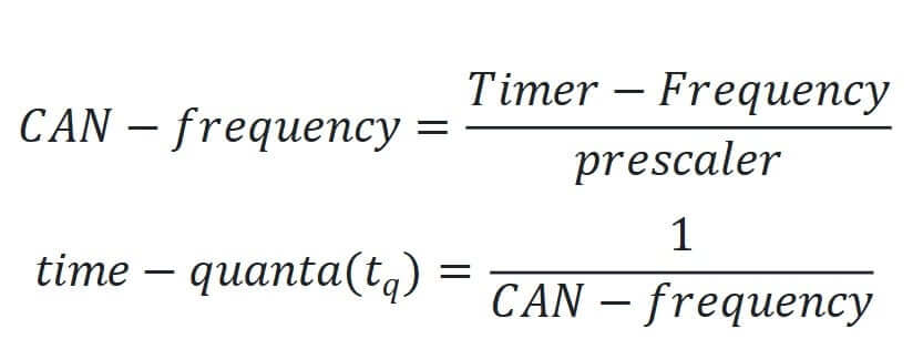
Our next task is to define the prescaler to set the CAN operating frequency. Please pay attention to the fact that we have a Nominal Prescaler and a Data Prescaler. As mentioned before, the STM32 FD CAN allows increasing the bit rate during the data transaction. The Nominal Prescaler dictates the frequency during the arbitration phase, while the Data Prescaler dictates the frequency during the data phase. In our case, I set both values to 32 to have 1.25 MHz in both cases. We call the reverse of this frequency a time quanta (Tq), which you might encounter in other technical documents.
So, the equations are:
The CAN Interface has no clock to synchronize the data segments. Hence, perfect timing is crucial for the proper operation of the bus. For that reason, the bit time is divided into different regions to adjust the sampling point of the data: Synchronization segment, Bit segment 1, and Bit segment 2. The synchronization segment points to the start of the bit time, and its duration is always a single time quanta (a single time quanta). Bit segment 1 (BS1, Phase segment 1 in STM32 CAN) defines the location of the sample point, while Bit segment 2 (BS2, Phase segment 2 in STM32 CAN) defines the location of the transmit point.
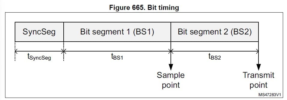
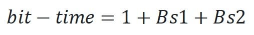
Do not be afraid of these technical words, because there are simple rules we can follow to configure their values. The sum of the data segments constitutes the duration of the data bit:
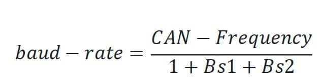
In other words, the baud rate equals:
Another rule of thumb is that the sample point (BS1 + 1) must be 80-90% of the bit time, which means BS1 is quite long compared to BS2. This is to ensure that sampling occurs after the data level has completely settled.
Another essential feature of the STM32 CAN is that nodes can adjust the bit timing dynamically to prevent data errors. The nodes' frequency values can vary slightly from one another, and the lengthening or shortening of the bit time is crucial to ensure the correct operation of the bus. The synchronization jump width (SJW) defines an upper bound for the amount of lengthening or shortening of the bit segments. It is programmable between one and four time quanta. The reference manual says:
"A valid edge is defined as the first transition in a bit time from dominant to recessive bus level, provided the controller itself does not send a recessive bit. If a valid edge is detected in BS1 instead of SYNC_SEG, BS1 is extended by up to SJW, thereby delaying the sample point. Conversely, if a valid edge is detected in BS2 instead of SYNC_SEG, BS2 is shortened by up to SJW, so that the transmit point is moved earlier."
Finally, I configured the bit timing parameters as shown in the figure below. The input clock frequency is 40 MHz, and the baud rate is 50 kbps for both the arbitration and data phases.
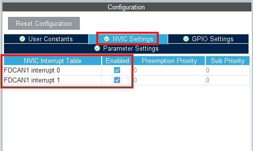
Finally, we need to enable the interrupt within the NVIC settings.
STM32 CAN Bus Course
STM32 CAN Bus Transmitting & Receiving Data in Real-time
We can generate the code after configuring the FD CAN and proceed to the next section of the tutorial: transmitting and receiving the frame.
First, within MX_FDCAN1_Init(), I define the Tx header:
Tx_header.Identifier = 0x77;
Tx_header.IdType = FDCAN_STANDARD_ID; // Satndard 11-bit ID
Tx_header.TxFrameType = FDCAN_DATA_FRAME; // Data Frame
Tx_header.DataLength = FDCAN_DLC_BYTES_12; // 12 bytes to send
Tx_header.ErrorStateIndicator = FDCAN_ESI_ACTIVE;
Tx_header.BitRateSwitch = FDCAN_BRS_OFF; // no bitrate switch
Tx_header.FDFormat = FDCAN_FD_CAN; // FD CAN
Tx_header.TxEventFifoControl = FDCAN_NO_TX_EVENTS;
Tx_header.MessageMarker = 0;
Within the main function, we start the CAN and enable the RX interrupt:
// main function
 if(HAL_FDCAN_Start(&hfdcan1)!= HAL_OK)
  {
	  Error_Handler();
  }
  if (HAL_FDCAN_ActivateNotification(&hfdcan1, FDCAN_IT_RX_FIFO0_NEW_MESSAGE, 0) != HAL_OK)
  {
    /* Notification Error */
    Error_Handler();
  }
After, I periodically send some dummy data through the CAN Interface:
  while (1)
  {
	  for (int i=0; i<12; i++)
	  {
	   Tx[i]++;
	  }

	  if (HAL_FDCAN_AddMessageToTxFifoQ(&hfdcan1, &Tx_header, Tx)!= HAL_OK)
	  {
	   Error_Handler();
	  }
	  HAL_Delay (1000);

    /* USER CODE END WHILE */

    /* USER CODE BEGIN 3 */
  }
Finally, I define the callback function and receive data:
void HAL_FDCAN_RxFifo0Callback(FDCAN_HandleTypeDef *hfdcan, uint32_t RxFifo0ITs)
{
  FDCAN_RxHeaderTypeDef   RxHeader;
  if((RxFifo0ITs & FDCAN_IT_RX_FIFO0_NEW_MESSAGE) != RESET)
  {
    /* Retrieve Rx messages from RX FIFO0 */
    if (HAL_FDCAN_GetRxMessage(hfdcan, FDCAN_RX_FIFO0, &RxHeader, Rx) != HAL_OK)
    {
    /* Reception Error */
    Error_Handler();
    }
    if (HAL_FDCAN_ActivateNotification(hfdcan, FDCAN_IT_RX_FIFO0_NEW_MESSAGE, 0) != HAL_OK)
    {
      /* Notification Error */
      Error_Handler();
    }
  }
} Also, do not forget to define some auxiliary variables:
uint8_t Tx[10];uint8_t Rx[10];
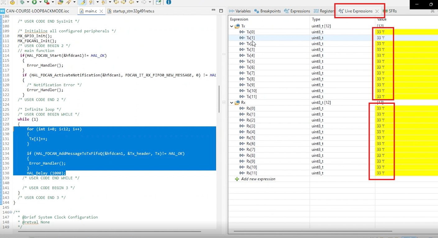
static FDCAN_TxHeaderTypeDef Tx_header; Finally, I will test this code by openning the debugging perspective. Within live expressions, I enter Rx and Tx to monitor the arrays in real time. When I press resume,
I can see how Rx buffer mirrors the values of Tx buffer, meaning that our LoopBack Mode works perfectly:
After the loopback mode is functional, we can move to the next part of the tutorial, when we start sending data between nodes,